2015-08-21
 496
496Semiconductor diodes are semiconductor devices which contain one rectifying and two non-rectifying junctions. The diode properties and characteristics are determined by a p-n junction. Let's recall the properties of a p-n junction. The p-n junction resistance depends on the current direction; namely:
-with the coinciding polarity majority carriers pass through the junction, the resistance is low and decreases with rising voltage;
-when the polarity is reversed, the resistance is high and does not depend on applied voltage.
This property of the p-n junction gives a possibility to create a great variety of semiconductor devices, the first in the list were rectifiers. The base of semiconductor diodes is a crystal of germanium or silicon.
Depending on their design semiconductor diodes may be classified into the so-called junction (alloyed) (Fig. 3.1) and point-contact diodes (Fig.3.2). The junction diodes are used to get high load currents and they operate within a low frequency range – 50Hz – 100 kHz. The point contact diodes are used in a high frequency range but for a low current. They have a low capacitance of a p-n junction.
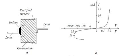
Fig.3.1. Germanium junction diode: a –structure, b – static characteristic curve
The structure of a germanium junction diode is shown schematically in Fig. 3.1a. It consists primarily of a germanium crystal which has electron conduction (n-type germanium) due to impurities antimony or arsenic added to it. The tin electrode (holder) is alloyed with the semiconductor at one side of the crystal. This electrode provides tight contact and permits an external circuit terminal to be connected. On the opposite side of the crystal the indium bar is alloyed with the semiconductor at the temperature about 5000C. Indium atoms penetrate into the semiconductor crystal, thus forming a hole conduction layer (p-type germanium) in it. Thus, a rectifying p-n junction is formed between the surface layer and the rest of the n-type germanium. The second terminal of the external circuit is soldered to the indium bar.
A characteristic curve of a germanium junction diode is shown in Fig. 3.1b. The plot of current as a function of voltage I=f (V) is called a static current-voltage characteristic. Devices which operate under Ohm’s law and have the plot I=f (V) as a straight line are called linear devices.
Semiconductor diodes are nonlinear devices. Their resistance depends on voltage or current that is why their characteristics are not a straight line. While considering this characteristic, it might be helpful to point out the following properties of the junction diode.
In the region of positive voltages (i.e., in the “forward” direction) current appears at low voltages (about 0.2-0.3V for germanium diodes and 0.6-0.7 V for silicon ones), and then rises abruptly. The forward resistance of a crystal diode is negligible, including the rectified current resistance in the positive region. In the region of negative voltages, the crystal diode still conducts a small current (due to minority carriers).
Under rising reverse voltage, reverse current is not at a steady level. It does not equal to saturated current I0 but slowly increases. At increasing reverse voltage the p-n-junction expands its own size and volume, thus, the number of generated charge carriers increases in a junction, and the thermal current of a junction IT also increases. The skin conduction of a p-n junction is the second reason for reverse current increasing. It defines a skin current Isk.